


With the unprecedented advancement in wireless technology, miniaturization, high reliability (stability), low cost, etc. have become essential feature for high end microwave devices. Wireless access applications that use 4th generation cell phones, blue-tooth enabled devices, wireless LAN, collision avoidance systems, millimeter wave radar, various antennas for optical communications and peripheral electronic devices demand materials with enhanced electrical performance. Among high performance materials, microwave substrates have a decisive role in improving the circuit density there by reducing the device size with multifunctional tasks. Filled PTFE substrates are ideal choice for microwave circuit fabrication owing to their exceptional electrical, mechanical and thermal properties. Though large volume of these materials is used for strategic as well as civil applications, currently the requirements are fully met through imports. To better serve the microwave designer needs, light weight, temperature stable and low loss microwave substrates are needed together with user defined dielectric constant which allow them to achieve high level of passive integration within a multilayer structure. In order to cater the requirement of microwave substrates indigenously, C-MET has developed a proprietary processing methodology comprising of Sigma Mixing, Extrusion, Calendering followed by Hot pressing (SMECH) process to fabricate planar, dimensionally stable and nearly isotropic PTFE/ceramic composite laminates. Chemical as well as Plasma etching have been employed to modify the surface of filled PTFE substrates for better adhesion with metal conducting layers. Copper cladding technology was established through vacuum lamination process to realize fine circuitry over flexible substrates.
Proprietary high dielectric microwave substrates have been developed for the first time, which are superior in properties compared to imported counterparts in terms of high dielectric constant (er up to 14.8), low loss tangent (tan d =0.002) and temperature stable microwave dielectric properties. One US and one Indian patent applications have been filed (US Patent application No. 14104002, 2013 and Indian Patent application No. 3815/DEL/2012) based on this innovation to protect the intellectual property right. The photographs of the indigenously developed microwave substrates and devices made out of them are given in Figs. 1-3.
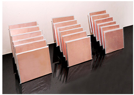
Fig. 1: 8”x8” size copper cladded high dielectric microwave substrate
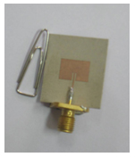
Fig. 2 : Miniaturized patch antenna fabricated using high dielectric substrates
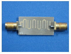
Fig. 3: Band pass filter fabricated using indigenous substrates
Ultra low loss tangent microwave substrates
C-MET has successfully developed ultra low loss microwave substrates with er=4.3±0.03 and loss tangent <0.0018 @ 10 GHz suitable for high power solid state amplifier design (Fig. 4). Using these indigenous microwave circuit boards, user agency (Raja Rammanna Centre for Advanced Studies) has fabricated high power solid state amplifiers (Fig. 5) operating at a center frequency of 505.8 MHz and installed the amplifiers in INDUS-2 at full rated power of 540 W(CW). Excellent RF performance was obtained in terms of output power, gain and efficiency during system level evaluation. In order to protect the intellectual property right, one US patent application (No. 14228342, 2014) has been filed to protect the intellectual property right of the innovation.
Fig. 4 Ultra low loss microwave printed circuit board developed at C-MET, Thrissur
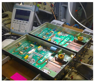
Fig. 5 High power solid state amplifiers fabricated using indigenous substrates
Temperature Stable Microwave substrates
The drift in operating frequency with respect to temperature is a serious problem while using flexible microwave substrates for outdoor wireless applications. C-MET has successfully designed, fabricated and tested ceramic filled PTFE substrates with temperature stable microwave dielectric properties for the first time using a single filler material. The temperature coefficient of dielectric constant of C-MET substrates is less than 30 ppm/oC in the temperature range -50 to 100oC.
Microwave Dielectric Resonators
Dielectric Resonator ( DR) is a ceramic compact, which can confine elecetromagnetic energy at microwave frequencies through total internal reflection by virtue of its high dielectric constant and high quality factor. High frequency devices such as satellite phones, global positioning systems, low noise oscillators, filters etc. have witnessed an explosive and an almost unprecedented growth in the recent years wherein dielectric resonators are used as the frequency determining component. In order to suit the aforementioned applications, a dielectric resonator should possess high dielectric constant ( er>20) for miniaturization, high unloaded quality factor ( Qu>2,000) for selectrivity and near zero temperature variation of resonant frequency ( tf≤20 ppm/oC) for sensitivity.
Super high Q Resonators
Barium Magnesium Tantalate ( BMT) has attractive microwave dielectric properties and it is considered to be an archetypal high Q dielectric resonator material. However, the processing of these materials is often difficult and yields a wide variation in their unloaded quality factors. Mostly, the quality factor of BMT material depends on the long range ordering of the B-site cations. Under Indigenization of Space Materials (ISM) programme, C-MET together with VSSC has successfully developed super high Q BMT microwave resonators through a simple and cost effective patented processing route (Indian Patent Application No. No. 2295/CHE/2009). The sintered BMT compacts exhibited a quality factor of 250000 GHz. BMT dielectric resonators were prepared in bulk quantities and space qualification tests have been performed to utilize these strategically important materials for satellite communication applications. The photograph of space qualified BMT ceramics is shown in Figure 6.
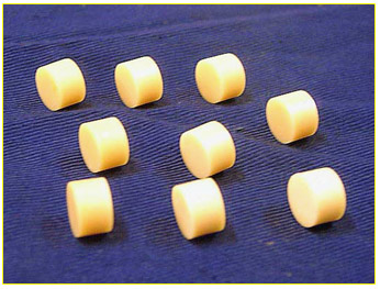
Fig. 6 Space qualified BMT ceramics
BMT technology was transferred to an Ahemedabad based industry viz. Sahajanand Laser Technologies Limited. The technology transfer agreement was signed by Dr. Koshy M. George, Deputy Director, VSSC and Dr. Kanhyalal, Director, RF & Microwave Division, Sahajanand Laser Technologies Limited on 25.05.2015 in a function held at VSSC, Thiruvannathapuram.
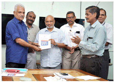
Fig. 7 Technology transfer of BMT ceramics
Ultra low temperature Co-fired Ceramics
Low-temperature cofired ceramic (LTCC) technology is a dominant approach used for multilayer circuit fabrication because of its high reliability and high integration of passive components. The vital features required for LTCC materials are low dielectric constant, high quality factor, low sintering temperature, and also chemical compatibility with metal electrodes. Most of the conventional microwave ceramics sinter at relatively high temperature (>1000°C), which restricts their wider usage in LTCC applications. Hence many material systems have been developed with sintering temperature less than 950oC so that Ag can be used as the metal electrode. The current trend is to further reduce the sintering temperature of microwave ceramic materials (<650oC) so that Al can be used an internal electrode. In this connection, C-MET has developed many novel vanadate and molybdate based ULTCC systems for multilayer circuit applications. The photograph of BaV2O6 ULTTC ceramic whocn can be sintered at 550 oC for 1 hr is give in Fig 8
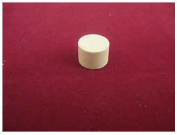
Fig. 8. Photograph of BaV2O6 ULTTC ceramics